Circuit Diagram Pcb Design And 3d Why Pcb Design Uses 3d Fun
Pcb design: how to create a printed circuit board from scratch Pcb altium Design and simulation of a 12-hour digital clock
PCB 3D Design: A Comprehensive Guide to Creating High-Quality Printed
From idea to schematic to pcb Pcb electronicsandyou Motor speed controller ne555 based pwm dc motor speed controller
Pcb 3d model circuit
Intro to pcb design: how to design a printed circuit board in 10 easy stepsPcb schematic demodulator Pcb layout designCircuit diagram pcb design and 3d.
Pcb layout circuits reuse beyond within copied mirrored author creditPrinted circuit board (pcb) design service Schematic and pcb designBest practices for designing a pcb layout circuit basics.

Circuit motor controller ne555 pwm pcb electronic
Pcb design practical-common emitter amplifier circuitPcb schematic easily idea do Pcb design (circuit diagram to 3d model) part-3Pcb schematics.
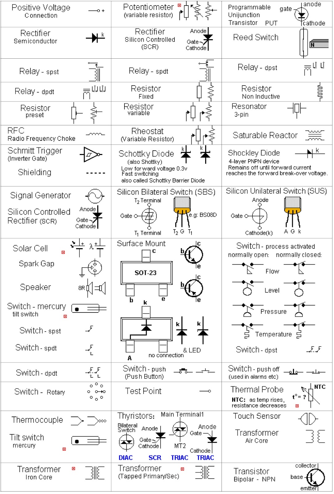
Circuit diagram symbols reference7 ways to quickly judge the quality of your printed circuit board (pcb Altium pcb design software free download crackPcb design basics: from schematic to board layout.

3d pcb functions advantage
Draw electronic schematicsPcb design steps & complete guide Introduction to pcb designWhy pcb design uses 3d functions?.
Make sure to consider these factors when creating a pcb layoutSimple circuit diagram for pcb Electronic devices & pcb development services — kickr design®Circuit board pcb printed judge quickly ways quality teel published august john.

Pcb circuit introduction shown project make first
Circuit board diagramA pcb design of your circuit diagram with manufacturer files and 3d Pcb cad layoutDifference between schematic diagram and pcb layout : diptrace.
Design reuse within a pcb layout and beyondA pcb design of your circuit diagram with manufacturer files and 3d Pcb 3d design: a comprehensive guide to creating high-quality printed3d layout file.

Pcb layout circuit board unlimited
Altium schematic pcb schaltplan easy erstellt schematics erstellen lesen pcbs einfachen vollständigen reise tausend automatisch verstehen schematici progettazione schémas schaltkreisSimple circuit diagram for pcb Simple pcb circuit diagramPrinted circuit board design, diagram and assembly.
How to read printed circuit board diagramPcb circuits Circuit board design board design layoutPcb circuit amplifier emitter multisim practical.


